A new era of faster, more efficient digital technology is closer thanks to research into the development of novel 2D materials in transistors.
Materials being developed by researchers at Nanjing University could allow more transistors to be squeezed on to chips, enabling faster, more powerful computers and new technologies. While the materials are still experimental, the researchers have overcome two key technical challenges that were preventing their use in transistors.
Developing novel transistor materials is a critical step towards achieving ‘beyond-silicon electronics’, which could add to silicon chips in everything from smartphones to cars. “There’s a limit for silicon transistors,” says Xinran Wang, an electrical engineer at Nanjing University, who led the research. “Beyond-silicon electronics is profoundly important as it stands to revolutionize technology and our daily lives.”
Moving beyond silicon is essential both for developing new devices such as flexible screens and super-efficient sensors and for realizing disruptive technologies such as quantum computing and artificial intelligence.

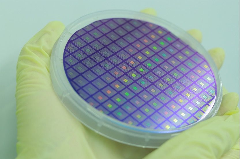
Novel transistors, such as the ones in this wafer-scale two-dimensional semiconductor ring oscillator circuit, will be critical for faster, more powerful computers.
Credit: Nanjing University
Silicon limit
For the past 60 years, the number of silicon transistors — the building blocks of integrated circuits — that can be squeezed on to a microchip has doubled every two years. This trend is known as Moore’s law. But the limit to this is fast approaching because, below a certain size, silicon transistors leak current, causing their efficiency to fall, and making the energy consumption of the chips “unacceptable,” Wang explains.
To solve this problem, Wang’s team is exploring the use of novel, non-silicon materials. These include ‘2D transition metal dichalcogenides’ (TMDs) such as molybdenum disulfide (MoS2) and tungsten diselenide (WSe2). Fashioning these compounds into three-atom-thick semiconductors could, in principle, make smaller and more energy efficient transistors, while avoiding the performance problems of silicon.
Wang’s team has been focusing on how to use these promising materials in workable devices.

Raw, uncut blue sapphires. Sapphire is an excellent electrical insulator, rigid and a good heat conductor, which makes it a promising base material on which to grow 2D materials for next generation transistors.
Credit: Shutterstock
One challenge is contact resistance. Occurring whenever materials with different electrical properties are physically joined, contact resistance impedes the flow of current, reducing the performance of transistors. Unlike silicon, TMDs do not form chemical bonds when they contact with metal electrodes, making it harder to transfer current and so increasing contact resistance.
“To tackle this, my students came up with a brilliant idea,” Wang says. They showed they could change the electrical interaction between the TMD and the metal by including an unusual phase of the semi-metal antimony in the metal electrode. This enhanced a property known as band hybridization, which increases the compatibility of two different conducting materials.
The increased band hybridization dramatically lowered the contact resistance. “The contact resistance is quite remarkable because it is lower than that of chemical-bonded contacts in silicon,” Wang says. The findings were reported in Nature in January 2023. TMD transistors constructed in this way could deliver a high current, with just a modest source-drain voltage — a performance that meets “beyond-silicon” roadmap targets set out by the Institute of Electrical and Electronics Engineers (IEEE), which develops global industry standards for electronics.
Building on sapphire
Research in Wang’s lab at Nanjing University has addressed another technical challenge to the use of TMD transistors. Most experts think that combining two layers of TMD would give better results and help TMD to outperform silicon. But these multilayer systems are difficult to prepare in a controlled way.
“Prior demonstrations were largely based on layer-by-layer growth, but they lacked a clear mechanism to precisely control layer thickness,” Wang says.
To address this problem, his team turned to the precious stone sapphire. They figured sapphire’s unusual combination of properties — excellent electrical insulation, rigid and a good heat conductor — could make it a useful base material on which to build layers of TMD of more uniform thickness.
In experiments, they showed that using sapphire allowed the growth of continuous and uniform films of bilayers of molybdenum disulfide (MoS2). “This has never been achieved before,” Wang says. The team reported their findings in Nature in 2022.
It’s a promising step forward, but Wang has worked to develop this technology since 2011 and he knows that the transition from laboratory prototypes to full-scale fabrication is not always easy. Still, he believes the Nanjing team is well placed to make more significant contributions.
“At this moment, we’re one of the very few teams worldwide that can cover the entire material–device–integration–equipment chain in the field of 2D semiconductors,” Wang says. “I’m proud that we’re doing great research in every direction.”
Future prospects
Wang is not ready to put a date on when this kind of technology will make it to real-world applications. But he is optimistic, because “most of the problems are technological rather than scientific.”
An important next step for the field is to develop reliable and cost-effective processes to manufacture large enough quantities of high-quality TMD materials. That will be crucial to compete with silicon chips, which can be made with near-perfect precision from sand.
Much of the progress so far has come from academic labs like Wang’s, but to take the next step, industry must get involved. That’s starting to happen, he says. “I’m very happy to see that many industrial leaders, including TSMC, Intel, IMEC and Samsung, are joining the party,” Wang says. “I’m optimistic that 2D materials will be part of our computer chips some day.”
References
Li, W. et al. Nature 613, 274–279, (2023). DOI 10.1038/s41586-022-05431-4
Liu, L. et al. Nature 605, 69–75, (2022). DOI: 10.1038/s41586-022-04523-5
Source: Office of Science and Technology


